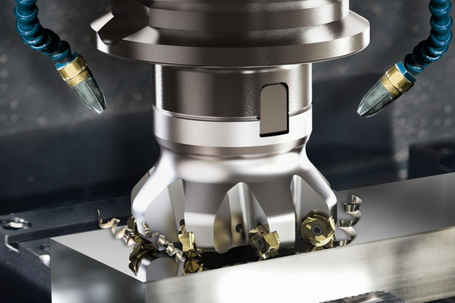
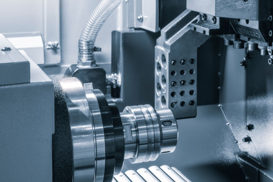
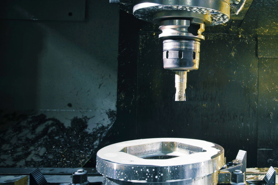
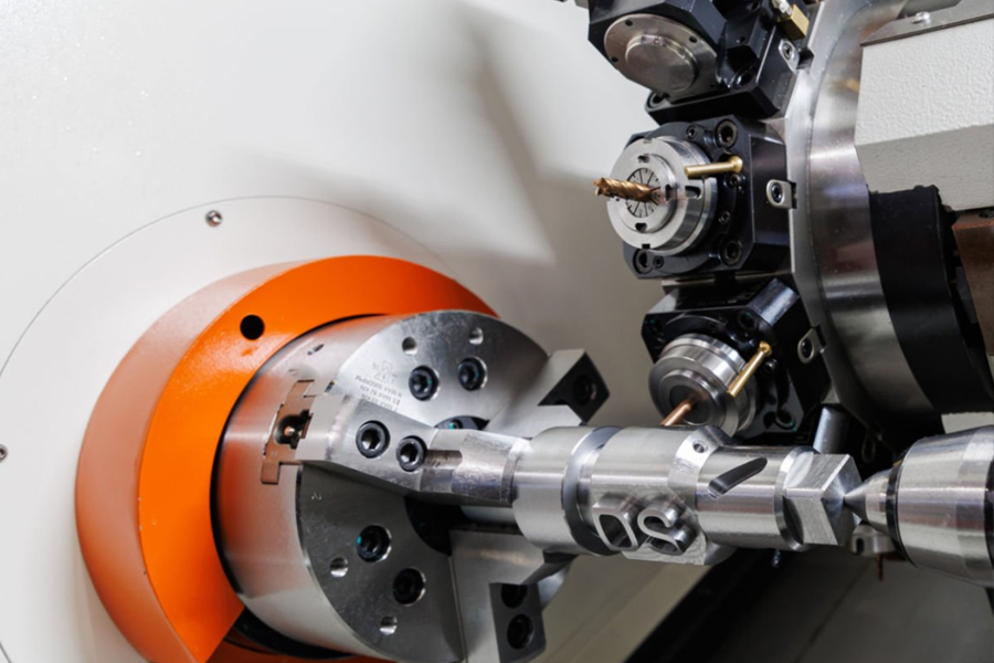
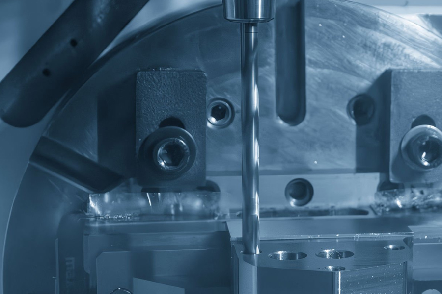
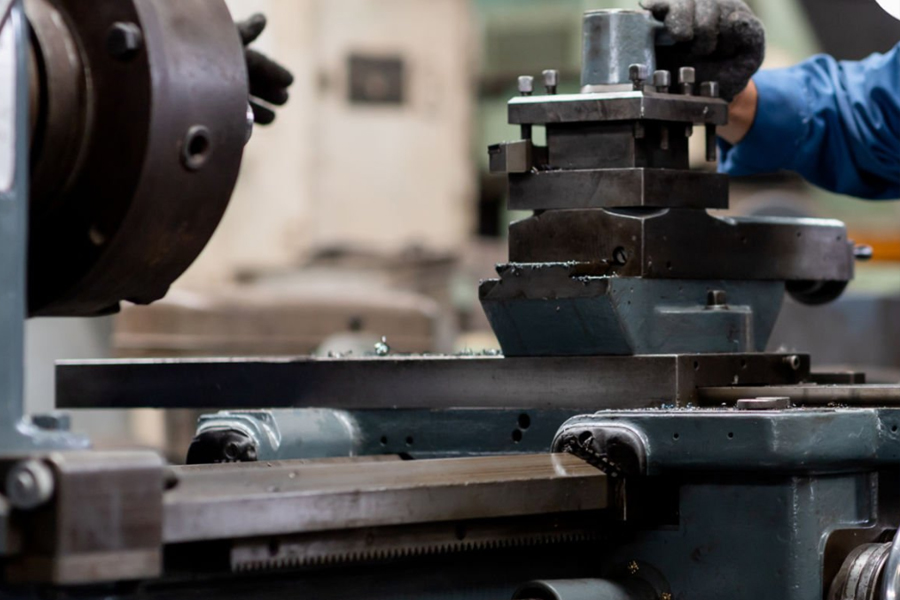
In today's era of rapid technological development, biosensors, as a key device that can accurately detect biological molecules, ions and other substances, are widely used in many fields such as medical diagnosis, environmental monitoring, and food safety testing. Taking medical parts processing as an example, biosensors play an irreplaceable role in early diagnosis of diseases and personalized medicine. The high precision and high sensitivity of biosensors are inseparable from advanced micro-nano manufacturing processes.
Photolithography process: fine drawing of microscopic patterns
Photolithography is a key step in the micro-nano manufacturing process of biosensors, similar to fine drawing in the microscopic world. Under the concept of CNC precision machining, the photolithography process uses photolithography equipment to transfer the designed circuit pattern to the substrate material through photoresist. First, a layer of photoresist is evenly applied on the surface of a pre-treated substrate, such as a silicon wafer. Photoresist is like a painter's canvas, waiting to be "drawn" with a precise pattern. Then, the mask is irradiated with a light source such as ultraviolet light, and the pattern on the mask will be projected onto the photoresist. After exposure, the chemical properties of the photoresist change. In the subsequent development process, the exposed part of the photoresist will be dissolved and removed, leaving a photoresist pattern on the substrate that is consistent with the mask pattern. The accuracy of this pattern can reach the micron or even nanometer level, laying the foundation for subsequent processing. For example, when manufacturing biosensors for detecting specific biomarkers, the photolithography process can accurately define the electrode pattern and microfluidic structure of the sensor, ensuring that the biomolecules can accurately interact with the recognition elements on the sensor surface and improve the accuracy of detection.
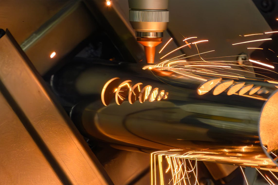
Etching process: the meticulous carving of the microscopic world
The etching process follows the photolithography step. It is like a master engraver in the microscopic world, further carving the pattern formed by photolithography. In the scope of precision machining, the etching process is mainly divided into wet etching and dry etching. Wet etching uses chemical solutions to selectively corrode the substrate material. For example, for a silicon substrate, a specific etching solution can be used to etch away the silicon material not protected by the photoresist, while retaining the silicon in the area covered by the photoresist, thereby forming the desired micro-nano structure. This method has a high etching rate and good isotropy, but there are certain challenges in controlling the etching accuracy. Dry etching etches the substrate with the help of plasma and other means. In the plasma environment, active ions react with the substrate material to achieve accurate removal of the material. Dry etching has higher etching accuracy and better anisotropy, and can produce more delicate and vertical microloan structures. In the processing of medical parts, for the microfluidic and nanoscale sensitive components of biosensors, the dry etching process can meet their strict requirements for high-precision structures.
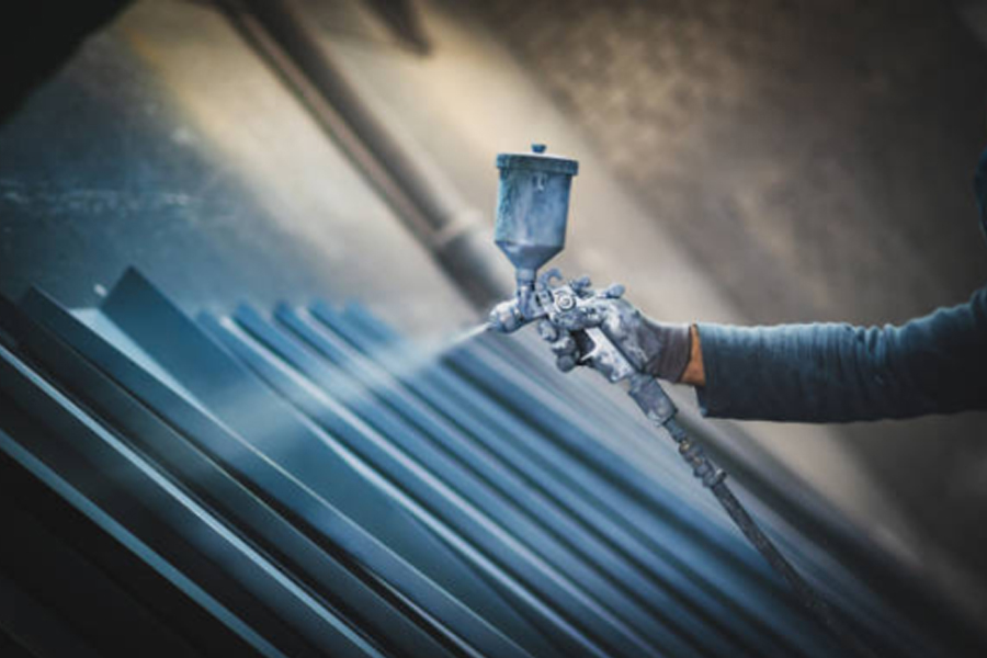
Coating process: giving sensors unique properties
The coating process also plays an indispensable role in the microloan manufacturing of biosensors. Through coating, one or more layers of thin films with specific functions can be added to the surface of the sensor to give the sensor unique properties. With the relevant technical support of CNC machining, commonly used coating methods include physical vapor deposition (PVD) and chemical vapor deposition (CVD). The PVD process forms a uniform film by evaporating metal or other materials and depositing them on the surface of the substrate. For example, a layer of gold film is plated on the surface of the biosensor. Gold has good conductivity and biocompatibility, which can improve the signal transmission efficiency of the sensor and provide an ideal surface for the fixation of biomolecules. The CVD process uses chemical reactions to generate thin films on the surface of the substrate. This method can produce high-quality films with precisely controlled components, which are suitable for manufacturing coatings with special functions, such as functional coatings used to improve the selective adsorption of specific biomolecules by sensors.
The micro-nano manufacturing process of precision machining of biosensors, through a series of delicate operations such as lithography, etching, and coating is like an exquisite artistic creation in the microscopic world, providing solid technical support for the high performance and miniaturization of biosensors, and promoting progress in many fields such as medicine and the environment.
